Silicon carbide (SiC), as a key material in the third-generation semiconductor industry, holds critical importance due to its superior thermal conductivity, high breakdown voltage, and wide bandgap. However, the conventional chemical mechanical polishing (CMP) process used in SiC wafer manufacturing is time-consuming and resource-intensive, involving significant material consumption and prolonged processing times. In this study, we explored the application of laser-assisted dry ablation as a pre-treatment for CMP. The experimental results showed that the single laser ablation depth of SiC is about 2 μm, and demonstrated that a laser spot overlap rate between 30% and 60% can generate a relatively lower surface roughness of SiC. This optimal range of overlap ensures a smoother ablation process, minimizing the irregularities on the SiC wafer surface. After a single pass of laser dry ablation, SiC hardness can be reduced to less than 3% of its original value, while material removal depth can be precisely controlled by adjusting the number of laser passes. With 50 repetitions, a material removal depth of nearly 30 μm was achieved. This reduction in hardness and enhanced material removal directly contribute to improve the efficiency of subsequent CMP processes by reducing polishing time and wear on grinding heads. In addition, after more than 5 times of laser treatment and then wet grinding, the thickness achievement rate can be increased from 73 to 93%. These results provide the important academic reference value. The integration of laser-assisted ablation into SiC wafer processing presents significant advantages in terms of increasing production throughput and reducing overall manufacturing costs. By simplifying the polishing steps and minimizing consumable usage, this approach offers a promising avenue for industrial applications, particularly in enhancing SiC wafer yield and optimizing semiconductor production workflows.
周老师: 13321314106
王老师: 17793132604


邮箱号码: lub@licp.cas.cn


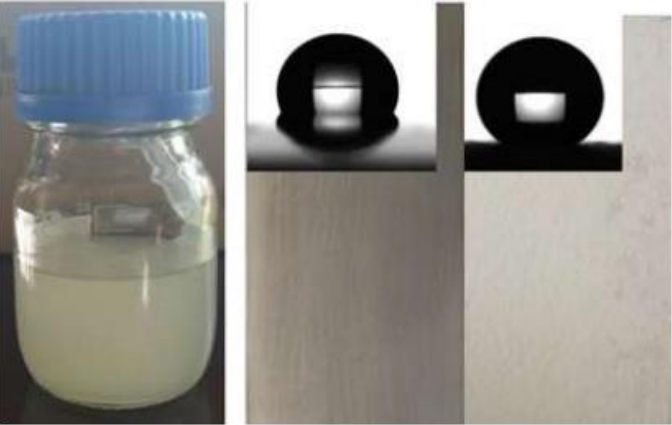
 润滑剂
润滑剂
 润滑油添加剂
 自润滑材料
自润滑材料
 密封材料
密封材料
 新兴材料
新兴材料
 加工设备
加工设备
 摩擦试验机
摩擦试验机
 大型表征仪器
 小型测试设备