Single-crystal wafers of p-type two-dimensional (2D) semiconductors are highly desired for next-generation electronics. However, p-type 2D semiconductors remain scarce, and achieving wafer-scale monolayer single crystals of such materials is even more challenging. Here we report the wafer-scale growth of p-type semiconducting monolayer MoSi2N4 single crystals on Cu (111) foils with prestored Mo and Si atoms. The <110> steps on Cu (111) guide the nucleation and unidirectional orientation of monolayer MoSi2N4 domains, enabling their seamless stitching into a continuous single-crystal film. The resulting MoSi2N4 exhibits exceptional quality, with an intrinsic mobility of 154 cm2 V−1 s−1. Field-effect transistor arrays fabricated from this material deliver excellent electrical performance, including an on/off ratio of ~3.8 ± 1.4 × 10⁶ and an on-state current density up to ~17.96 μA μm−1 (1 μm channel length), along with superior stability compared with monolayer WSe2-based counterparts. Furthermore, this versatile growth strategy also enables the fabrication of wafer-scale monolayer WSi2N4 single crystals. This work establishes a promising p-type 2D semiconductor platform for future integrated circuits.
周老师: 13321314106
王老师: 17793132604


邮箱号码: lub@licp.cas.cn




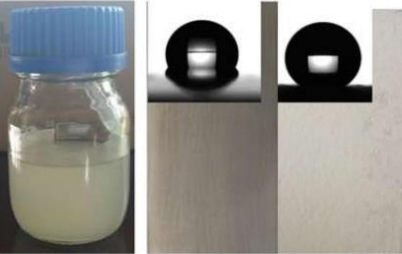
 润滑剂
润滑剂
 润滑油添加剂
 自润滑材料
自润滑材料
 密封材料
密封材料
 新兴材料
新兴材料
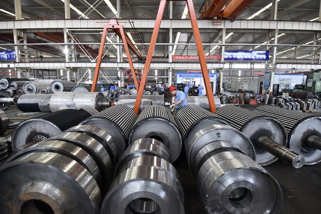 加工设备
加工设备
 摩擦试验机
摩擦试验机
 大型表征仪器
 小型测试设备